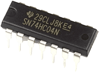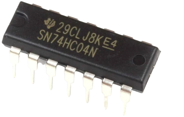


7404 NOT Gate IC
Product Details
Number of Gates: The 7404 IC contains six NOT gates. This means you have six independent logic gates in a single package.
Pin Configuration: The pinout of a typical 7404 IC is as follows:
- Pins 1: Input (A) for the first inverter.
- Pins 2: Output (Y) for the first inverter.
- Pins 3: Input (A) for the second inverter.
- Pins 4: Output (Y) for the second inverter.
- Pins 5: Input (A) for the third inverter.
- Pins 6: Output (Y) for the third inverter.
- Pins 7: Input (A) for the fourth inverter.
- Pins 8: Output (Y) for the fourth inverter.
- Pins 9: Input (A) for the fifth inverter.
- Pins 10: Output (Y) for the fifth inverter.
- Pins 11: Input (A) for the sixth inverter.
- Pins 12: Output (Y) for the sixth inverter.
- Pins 13: Supply voltage (VCC).
- Pins 14: Ground (GND).
Truth Table: The truth table for a NOT gate is simple:
Input (A) Output (Y) 0 1 1 0 In this truth table, "0" represents a logic low or "false," while "1" represents a logic high or "true."
Operation: The NOT gate (inverter) performs a logical negation on its input. The output is the opposite of the input. If the input is "0," the output is "1," and if the input is "1," the output is "0."
Note: You can use the 7404 IC to perform logical inversion operations, signal buffering, and logic level conversion. It's a fundamental building block in digital electronics and is commonly used in various digital circuits.


