
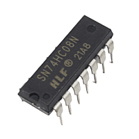
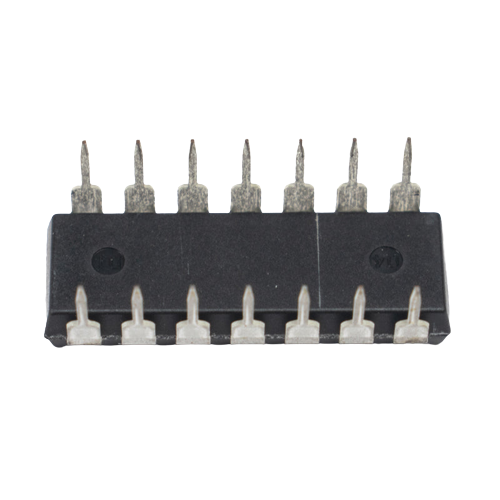
7408 AND Gate IC
Product Details
Number of Gates: The 7408 IC contains four AND gates. This means you have four independent logic gates in a single package.
Pin Configuration: The pinout of a typical 7408 IC is as follows:
- Pins 1 and 2: Inputs (A and B) for the first AND gate.
- Pins 3: Output (Y) for the first AND gate.
- Pins 4 and 5: Inputs (A and B) for the second AND gate.
- Pins 6: Output (Y) for the second AND gate.
- Pins 7 and 8: Inputs (A and B) for the third AND gate.
- Pins 9: Output (Y) for the third AND gate.
- Pins 10 and 11: Inputs (A and B) for the fourth AND gate.
- Pins 12: Output (Y) for the fourth AND gate.
- Pins 13: Supply voltage (VCC).
- Pins 14: Ground (GND).
Truth Table: The truth table for a 2-input AND gate is as follows:
Input A Input B Output (Y) 0 0 0 0 1 0 1 0 0 1 1 1 In this truth table, "0" represents a logic low or "false," while "1" represents a logic high or "true."
Operation: The AND gate performs a logical AND operation on its inputs. The output is "1" (logic high) only when both inputs are "1" (logic high). In all other cases, the output is "0" (logic low).
Note: You can use the 7408 IC to implement various logic functions and construct digital circuits. It's a fundamental building block in digital electronics and is commonly used for tasks such as logical conjunction, signal multiplexing, and logic level conversion.


